


 |
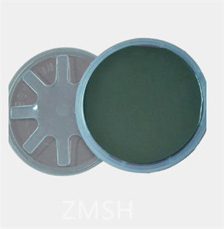
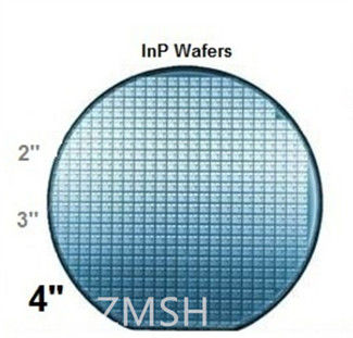
3inch InP Indium Phosphide Substrate N-Type Semiconductor VGF Growth Method 111 100 Orientation
Product Details:
| Place of Origin: | China |
| Brand Name: | ZMSH |
Payment & Shipping Terms:
| Delivery Time: | 2-4 weeks |
|---|---|
| Payment Terms: | T/T |
|
Detail Information |
|||
| Size (inch): | 3” | Thickness (μm): | 600± 25 |
|---|---|---|---|
| Dopant: | Iron (N Type) | Polished: | Single Side |
| Mobility: | (1.5-3.5)E3 | Orientation: | 111 |
| EPD: | ≤5000 | Growth Method: | VGF |
| IF Length: | 11±1 | ||
| High Light: | VGF growth method Indium Phosphide Substrate,111 100 orientation Indium Phosphide Substrate,N-Type Semiconductor Indium Phosphide Substrate |
||
Product Description
3inch InP Indium Phosphide Substrate N-Type Semiconductor VGF growth method 000 001 orientation
Product abstract
Our InP (Indium Phosphide) products offer high-performance solutions for a variety of applications in the telecommunications, optoelectronics, and semiconductor industries. With superior optical and electronic properties, our InP materials enable the development of advanced photonic devices, including lasers, photodetectors, and optical amplifiers. Whether you need substrates, epitaxial wafers, or custom-designed components, our InP products deliver reliability, efficiency, and precision for your demanding photonics projects.
Product showcase
![]()
Product properties
-
High Optical Transparency: InP exhibits excellent optical transparency in the infrared region, making it suitable for various optoelectronic applications.
-
Direct Bandgap: The direct bandgap nature of InP allows for efficient light emission and absorption, making it ideal for semiconductor lasers and photodetectors.
-
High Electron Mobility: InP offers high electron mobility, enabling fast charge carrier transport and facilitating high-speed electronic devices.
-
Low Thermal Conductivity: InP's low thermal conductivity helps in efficient heat dissipation, making it suitable for high-power optoelectronic devices.
-
Chemical Stability: InP demonstrates good chemical stability, ensuring the long-term reliability of devices even in harsh operating environments.
-
Compatibility with III-V Compound Semiconductors: InP can be seamlessly integrated with other III-V compound semiconductors, allowing for the development of complex heterostructures and multifunctional devices.
-
Tailorable Bandgap: The bandgap of InP can be engineered by adjusting the phosphorus composition, enabling the design of devices with specific optical and electronic properties.
-
High Breakdown Voltage: InP exhibits high breakdown voltage, ensuring the robustness and reliability of devices in high-voltage applications.
-
Low Defect Density: InP substrates and epitaxial layers typically have low defect densities, contributing to high device performance and yield.
-
Environmental Compatibility: InP is environmentally friendly and poses minimal risks to health and the environment during manufacturing and operation.
-
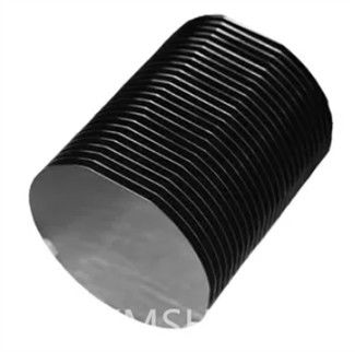
Parameter 2” S-doped InP Wafer 2” Fe-doped InP Wafer Material VGF InP Single Crystal Wafer VGF InP Single Crystal Wafer Grade Epi-Ready Epi-Ready Dopant S Fe Conduction Type S-C-N S-I Wafer Diameter (mm) 50.8±0.4 50.8±0.4 Orientation (100) º±0.5º (100)º±0.5º OF location / Length EJ [0-1-1] / 17±1 EJ [0-1-1] /17±1 IF Location / Length EJ [0-1 1] / 7±1 EJ [0-1 1] / 7±1 Carrier Conc. (cm-3) (1~6) E 18 1.0E7 - 5.0E8 Resistivity (Wcm) 8~15 E-4 ≥1.0E7 Mobility (cm2/Vs) 1300 ~ 1800 ≥2000 Average EPD (cm-2) ≤ 500 ≤ 3000 Thickness (µm) 475 ± 15 475 ± 15 TTV/TIR (µm) ≤15 ≤15 Bow (µm) ≤15 ≤15 Wrap (µm) ≤15 ≤15 Particle Count N/A N/A Surface Front side: Polished,
Black side: EtchedFront side: Polished,
Black side: EtchedWafer Packaging Wafer fastened by a spider in an individual tray and sealed with N2 in a static shielding bag. Packing done in a class 100 clean room. Wafer fastened by a spider in an individual tray and sealed with N2 in a static shielding bag. Packing done in a class 100 clean room -
Product applications
-
Telecommunications: InP-based devices are widely used in telecommunications networks for high-speed data transmission, including optical fiber communication systems and high-frequency wireless communication.
-
Photonics: InP materials are essential for the development of various photonic devices, such as semiconductor lasers, photodetectors, modulators, and optical amplifiers, used in telecommunications, sensing, and imaging applications.
-
Optoelectronics: InP-based optoelectronic devices, such as light-emitting diodes (LEDs), laser diodes, and solar cells, find applications in displays, lighting, medical equipment, and renewable energy systems.
-
Semiconductor Electronics: InP substrates and epitaxial layers serve as platforms for the fabrication of high-performance transistors, integrated circuits, and microwave devices for radar systems, satellite communications, and military applications.
-
Sensing and Imaging: InP-based photodetectors and imaging sensors are utilized in various sensing applications, including spectroscopy, lidar, surveillance, and medical imaging, due to their high sensitivity and fast response time.
-
Quantum Technology: InP quantum dots and quantum wells are explored for their potential applications in quantum computing, quantum communication, and quantum cryptography, offering advantages in coherence and scalability.
-
Defense and Aerospace: InP devices are deployed in defense and aerospace systems for their reliability, high-speed operation, and radiation hardness, supporting applications such as radar systems, missile guidance, and satellite communication.
-
Biomedical Engineering: InP-based optical sensors and imaging systems are employed in biomedical research and clinical diagnostics for non-invasive monitoring, imaging, and spectroscopic analysis of biological samples.
-
Environmental Monitoring: InP-based sensors are utilized for environmental monitoring applications, including pollution detection, gas sensing, and remote sensing of atmospheric parameters, contributing to environmental sustainability efforts.
-
Emerging Technologies: InP continues to find applications in emerging technologies such as quantum information processing, silicon photonics integration, and terahertz electronics, driving advancements in computing, communication, and sensing.
-