


 |
Silicon Wafer 4 Inch Thickness 500+/-20 Resistivity 1-10 Ohm·cm Orientation100 Double Side Polish
Product Details:
| Place of Origin: | China |
| Brand Name: | ZMSH |
| Model Number: | si wafer |
Payment & Shipping Terms:
| Payment Terms: | T/T |
|---|
|
Detail Information |
|||
| Growing Method: | FZ | Orientation: | <111> |
|---|---|---|---|
| Off-orientation: | 4±0.5 Degree To The Nearest <110> | Type/Dopant: | P/Boron |
| Resistivity: | 10-20 W.cm | RRV: | ≤15% (Max Edge-Cen)/Cen |
| TTV: | ≤5 Um | Bow: | ≤40 Um |
| Warp: | ≤40 Um | ||
| High Light: | Orientation100 Silicon wafer,500+/-20 Resistivity Silicon wafer,4 inch thickness Silicon wafer |
||
Product Description
Silicon wafer 4 inch thickness 500+/-20 Resistivity 1-10 ohm·cm Orientation100 double side polish
Product abstract
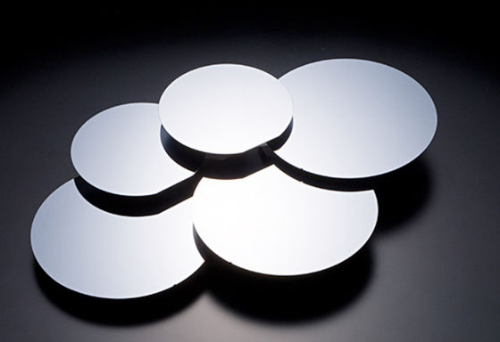
![]()
Our Precision Ultra-Pure Silicon Substrate is meticulously engineered to serve as the foundation for high-performance semiconductor devices. Crafted with advanced float-zone mono-crystalline silicon technology, this substrate offers exceptional purity and uniformity, ensuring superior electronic properties. With precise control over crystal structure and impurity levels, our substrate enables the fabrication of cutting-edge semiconductor devices with enhanced reliability and performance. Whether used in integrated circuits, power electronics, or photovoltaic applications, our silicon substrate empowers innovation across various industries, driving advancements in technology and engineering.
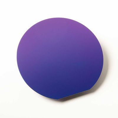
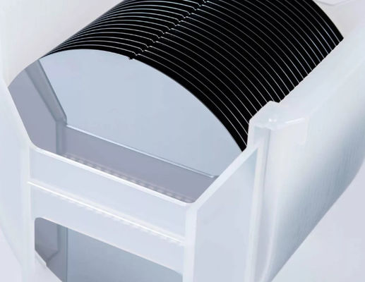
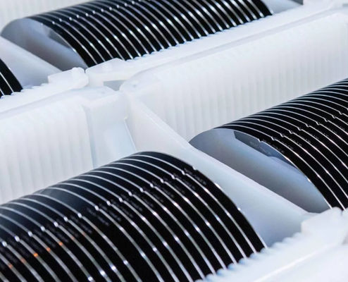
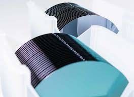
Product showcase
![]()
![]()
Product properties
-
Ultra-Pure Silicon: Our substrate is composed of float-zone mono-crystalline silicon, ensuring exceptional purity levels crucial for high-performance semiconductor devices.
-
-
Uniform Crystal Structure: The substrate boasts a uniform crystal structure, free from defects or irregularities, ensuring consistent electrical properties across the entire surface.
-
-
Low Impurity Levels: With meticulous control over impurity concentrations, our substrate exhibits low levels of dopants and contaminants, minimizing unwanted electronic effects and ensuring device reliability.
-
-
High Thermal Stability: The substrate demonstrates high thermal stability, enabling reliable operation across a wide range of temperatures without compromising performance or integrity.
-
-
Precise Dimensional Control: Each substrate is manufactured with precise dimensional control, ensuring consistent thickness and flatness to facilitate accurate device fabrication processes.
-
-
Excellent Surface Quality: Our substrate features a smooth and defect-free surface finish, essential for the deposition of thin films and the formation of high-quality device interfaces.
-
-
Customizable Specifications: We offer a range of customizable specifications, including doping concentration, resistivity, and orientation, to meet the specific requirements of diverse semiconductor applications.
-
-
Compatibility with Semiconductor Processes: The substrate is compatible with various semiconductor processing techniques, including epitaxy, lithography, and etching, enabling seamless integration into existing fabrication workflows.
-
-
Electrical Performance: Our substrate exhibits excellent electrical properties, including high carrier mobility, low leakage currents, and uniform electrical conductivity, essential for optimizing device performance and efficiency.
-
-
Reliability and Longevity: Designed for long-term reliability, our substrate undergoes rigorous quality control measures to ensure consistent performance and durability throughout its operational lifespan.
-
FZ monocrystalline silicon specification
Type Conduction Type Orientation Diameter(mm) Conductivity(Ω•cm) High resistance N&P <100>&<111> 76.2-200 >1000 NTD N <100>&<111> 76.2-200 30-800 CFZ N&P <100>&<111> 76.2-200 1-50 GD N&P <100>&<111> 76.2-200 0.001-300 Wafer specification
Ingot Parameter Item Description Growing method FZ Orientation <111> Off-orientation 4±0.5 degree to the nearest <110> Type/Dopant P/Boron Resistivity 10-20 W.cm RRV ≤15% (Max edge-Cen)/Cen Wafer Parameter Item Description Diameter 150±0.5 mm Thickness 675±15 um Primary Flat Length 57.5±2.5 mm Primary Flat Orientation <011>±1 degree Secondary Flat Length None Secondary Flat Orientation None TTV ≤5 um Bow ≤40 um Warp ≤40 um Edge Profile SEMI Standard Front Surface Chemical-Mechenical Polishing LPD ≥0.3 um@≤15 pcs Back Surface Acid Etched Edge Chips None Package Vacuum Packing; Inner Plastic, Outer Aluminum -
Product applications
Integrated Circuits (ICs): Our precision ultra-pure silicon substrate serves as a fundamental building block for the fabrication of ICs used in a wide range of electronic devices, including smartphones, computers, and automotive electronics.
Power Electronics: The substrate is utilized in power semiconductor devices such as diodes, transistors, and thyristors, enabling efficient energy conversion and control in applications such as electric vehicles, renewable energy systems, and industrial automation.
Photovoltaics (PV): Our substrate plays a crucial role in the manufacturing of high-efficiency solar cells, providing a stable and uniform base for the deposition of semiconductor layers and metal contacts, leading to improved solar energy conversion efficiency.
Light-Emitting Diodes (LEDs): In LED manufacturing, our substrate serves as a platform for epitaxial growth of semiconductor layers, ensuring uniformity and reliability in LED performance for applications such as lighting, displays, and automotive lighting.
Microelectromechanical Systems (MEMS): Our substrate facilitates the fabrication of MEMS devices, including accelerometers, gyroscopes, and pressure sensors, enabling precise sensing and control in consumer electronics, automotive systems, and medical devices.
Radio Frequency (RF) Devices: The substrate is used in the production of RF devices such as RF amplifiers, oscillators, and filters, supporting wireless communication systems, satellite communication, and radar systems with high-frequency operation and reliability.
Optoelectronic Devices: Our substrate enables the development of optoelectronic devices such as photodetectors, optical modulators, and laser diodes, contributing to applications in telecommunications, data communication, and optical sensing.
Biomedical Sensors: In biomedical engineering, our substrate is employed for the fabrication of biosensors and bioelectronic devices for applications such as medical diagnostics, drug delivery systems, and implantable medical devices.
Aerospace and Defense: The substrate is utilized in aerospace and defense applications, including radar systems, communication satellites, and missile guidance systems, where reliability, stability, and performance are critical in harsh environments.
Emerging Technologies: Our substrate supports advancements in emerging technologies such as quantum computing, neuromorphic computing, and advanced sensors, driving innovation in computing, artificial intelligence, and sensing applications.